R&D

We introduce you to the R&D
of SEVENENG, Co., Ltd., a reliable company to entrust.
We are a venture business that develops and manufactures dies and jigs used in cameras/computers/medical equipment. We manufacture our products with highest technologies and select quality.
R&D
- SUS automatic tack welding Die (completed in 2016)
- Rigid-Flex shearing Die
- Jig developed with new materials
- Development of technology of after-treatment process of new material jigs.
- Technical data sheet
-
-
Enhanced the workability and productivity of the FPCB manufacturing process
-
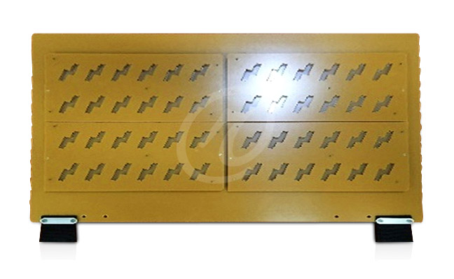
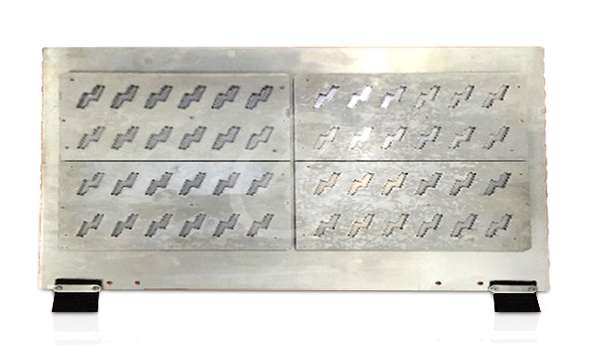
FPCB magnesium alloy JIG
-
-
Characteristics by materials
-
Material characteristics Bakelite Aluminum Magnesium Density
(density, g/cm3)~1.8 2.70 1.78 Specific heat capacity
(specific heat capacity, J/cm3·K)0.92 2.42 1.78 Thermal conductivity
(thermal conductivity, W/m·K)0.2 167 96 * Destructive temperature
(℃)120~140 - - Melting point
(melting temperature, ℃)- 646 632 Tensile strength
(tensile strength, MPa)~50 310 266 -
· The temperature at which the material starts carbonization, collapse, and melts
-
-
Bakelite Jig 500 x 450
3.78 kg -
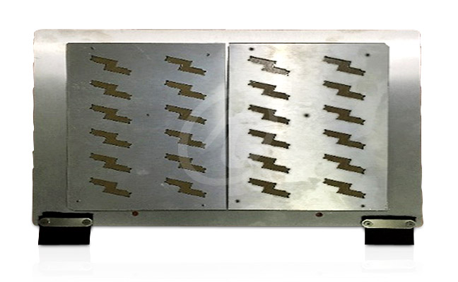
Al Jig 500 x 450
5.64 kg -
Mg Jig 500 x 450
3.72 kg
-
-
Weight is the same as that of bakelite Jig and precision and thermal characteristics are superior that those of the aluminium jig.
-
-

-
Development of magnesium alloy jig for manufacture of FPCB.
-
- Development of magnesium alloy jig production for hot press equipment.
- Optimization of the after-treatment process of magnesium alloy fabrication.
- Currently the development of process condition optimization technology for surface treatment of magnesium alloy jig is under way.
- Currently the development of process technology for the after-treatment of magnesium alloy jig is under wat.
-
-
-
TOOL TYPE
-
Major classification Sub-classification 1 Sub-classification 2 TOOL HARD TOOL PIERCING COMPOUND KNOCK-OUT TYPE PUSH BACK TYPE SOFT TOOL WOOD Wooden pattern TYPE PVC(Sealing) TYPE PINNACLE ROTARY -
· Others : TRIM Die, automatic tack welding Die, AUTO Die, Drawing & redrawing Die, Progressive Die, MOLD & CONNECTOR Die.
-
Die(HARD TOOL)
-
What is a Die?
- A metallic shape made to manufacture products of the same scale in massive volume.
-
Needs for Die
- It gives dimensional precision to products and parts manufactured.
- Because of the same dimensions of products made using it, products are compatible and it is easy to assemble the parts.
- The appearance of the products are neat and it is easy to change models.
- It is possible to produce a product without special technique or skills.
- The time for producing a product is reduced.
-
Kinds of Die
HARD TOOL PIERCING Sub-materials(COVERLAY,P.P,BOND...): mainly used for punch out and after fabrication of the routing (punching out), useless parts are sheared and the useful parts the only are left with the product. COMPOUND KNOCK-OUT Used for routing and is a fabrication method where the product that gets off from the workpiece that was inserted between upper PAD and IDE and was slided vertically is received using a knockout cylinder. PUSH BACK Used for routing and, different from the knockout operation method, a method of fabrication where the workpiece is inserted into a panel or block again at the same time it is punched out (the inspection of the next operation is easy).
-
Die structure
-

-
Principles of Die press
-
-

First phase : Plastic deformation occurs. Plastic deformation occurs on the product.
-
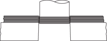
Second phase : Penetration phase Deformation of the product(shearing) starts.
-
Third phase : Failure phase. Failure occurs between the PUNCH and the shearing edge of the DIE.
-
-
What is FPCB(FLEXIBLE PRINTED CIRCUITS BOARD)?
-
- An electronic part that was developed to respond to the trends of miniaturization and complexification of electronic parts and which has a good workability, and superior heat-resisting property, bending-resistance, chemical-resistance shows less variability of dimensions, strong at heat, and it takes less time in assembly of products made from it.
- This is widely used as a critical parts in such electronic products camera, computer and it peripherals, PRINTER, HANDPHONE, VIDEO & AUDIO device, CAMCORDER, DVD, TFT LCD, satellite devices, military equipment and medical equipment.
-
Advantages of FPCB
-
- It is possible to three-dimensional wiring without any other support. It is possible to realize minimization and weight-reduction of appliances.
- It is possible to wiring with high-durability and high-density upon repeatedly flexed surfaces(0.2m/m pitch)
- There is no error in wiring and the assembly operation is easy and highly reliable. Repetitive production mode is possible.
-
Overview of FPCB
-
Function A part of electronic appliance used to mount electronic parts and connect among those parts electrically. Emergence Since the US NBS(National Bureau Standard) has used the vacuum tube as an active element and formed an circuit of resisters, condensers and coils connected a printed circuit on the insulated board to minimization of electronic devices in 1947, the current form of PCB has emerged. Characteristics · It became the basic parts of all electronic products.
· It is a kind of complex set of technologies such as mechanics, electronics, chemicals, metallics, etc.
· It is a critical part that leads the development of IT industry.
· As it is an equipment industry, it requires precision in timing of investment and scale.
· The business is affected by environmental factors such as business cycle of the electronics industry.Trends Minimization and high-functionalization of electronics part.
→ Trends of high-density and multi-layerization of PCB materials / manufacturing process (Substrate/Build-up)
-
Classification of FPCB
-
Single-face PCB
(Single Side PCB)· PCB for which the circuit is formed on only one face.
· Mounting density is low and manufacturing process is simple.
· Used in: Mass production items such home appliance products as TV, VTR, AUDIO, refrigerator.Dual-face PCB
(Double Side PCB)· PCB for which the circuit are formed on the two faces, upper and lower side.
· It is possible to mount parts in higher density compared to single-face PCB.
· Used in: low function OA devices such ad PRINTER, FAX and low price industrial devices.Multi-layer PCB
(Multi Layer Board)· Three-dimensional PCB which has internal and external circuits.
· Using three dimensional wiring, it is possible to mount parts in higher density.
· Used in: Large computers, PC, communication devices, small home appliances.Special PCB ① IVH PCB (Interstitial Via Hole PCB)
· PCB where partial vial holes are fabricated so that selective circuit connection is possible by layer.
· Used in: High function small electronic devices such as obile phone, notebook PC, PDA etc.
② BGA PCB (Ball Grid Array PCB)
· PCB for use in a packaged product that is designed to mount the Solder Ball that was attached to the under-side of a sub-board for packaged product on which Bare Chip is mounted.
③ R-F PCB (Rigid-Flex PCB)
· For maximum use of limited device space and enhancement of reliability of connection, connect between rigid MLB structures using integrated Flex PCBs.
-
FPCB manufacturing process (MLB-basis)
-
-
01 Cuttiing
Cuts raw materials (Core) into panel sizes suitable for processing. -
02 Formation of internal layers
Form circuits on the internal materials(exposure to light, development, corrosion, flaking) -
03 Lamination
Conjugate internal raw material in which the circuit is formed and the insulator layer in high temperature. -
04 CNC Drill
Hole fabrication for the interconnection between layers. -
05 Copper plating
By plating the holes with copper, connect external layer and internal layer. -
06 Formation of the external circuit
Form external circuit on the copper plated external layer (exposure to light, development, corrosion, flaking) -
07 Printing
Apply inalterable ink for the purpose of circuit protection. -
08 Surface treatment
Surface treatment for the prevention of oxidization of the copper plate where ink is not applied. -
09 Routing (External shape processing)
Route the panel in sizes that are required by customers. -
10 B.B.T
Inspection to find out electrical defects. -
11 Final inspection
A total inspection to find out defects in appearance using magnifying glass. -
12 Shipment test
Inspect appearance defects/dimension defects through sampling. -
13 Packaging
Package the product using vacuum packing and buffer materials.
-
-


